


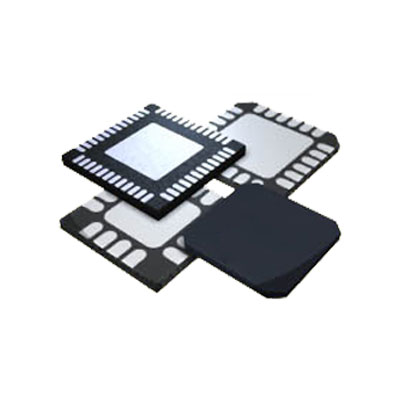


AD9258-105BCPZ Product Details
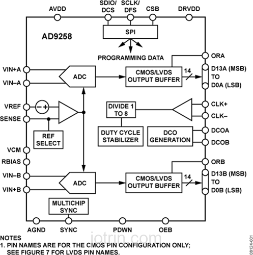
The dual ADC core features a multistage, differential pipelined architecture with integrated output error correction logic. Each ADC features wide bandwidth differential sample-and-hold analog input amplifiers that support a variety of user-selectable input ranges. An integrated voltage reference eases design considerations. A duty cycle stabilizer is provided to compensate for variations in the ADC clock duty cycle, allowing the converters to maintain excellent performance.
The ADC output data can be routed directly to the two external 14-bit output ports. These outputs can be set to either 1.8 V CMOS or LVDS.
Flexible power-down options allow significant power savings, when desired.
Programming for setup and control is accomplished using a 3-wire SPI-compatible serial interface.
The AD9258 is available in a 64-lead LFCSP and is specified over the industrial temperature range of −40°C to +85°C.
Product Highlights
Feature
- SNR = 77.6 dBFS @ 70 MHz and 125 MSPS
- SFDR = 88 dBc @ 70 MHz and 125 MSPS
- Low power: 750 mW @ 125 MSPS
- 1.8 V analog supply operation
- 1.8 V CMOS or LVDS output supply
- Integer 1-to-8 input clock divider
- IF sampling frequencies to 300 MHz
- −152.8 dBm/Hz small signal input noise with 200 Ω input impedance @ 70 MHz and 125 MSPS
- Optional on-chip dither
- Programmable internal ADC voltage reference
- Integrated ADC sample-and-hold inputs
- See data sheet for additional features
Applications
- Communications
- Diversity radio systems
- Multimode digital receivers (3G) GSM, EDGE, W-CDMA, LTE, CDMA2000, WiMAX, TD-SCDMA
- I/Q demodulation systems
- Smart antenna systems
- General-purpose software radios
- Broadband data applications
- Ultrasound Equipment
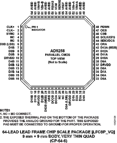
(Picture: Pinout)
(Picture: Diagram)